- 您现在的位置:买卖IC网 > Sheet目录443 > IRF6614TR1 (International Rectifier)MOSFET N-CH 40V DIRECTFET-ST
�� �
�
�IRF6614�
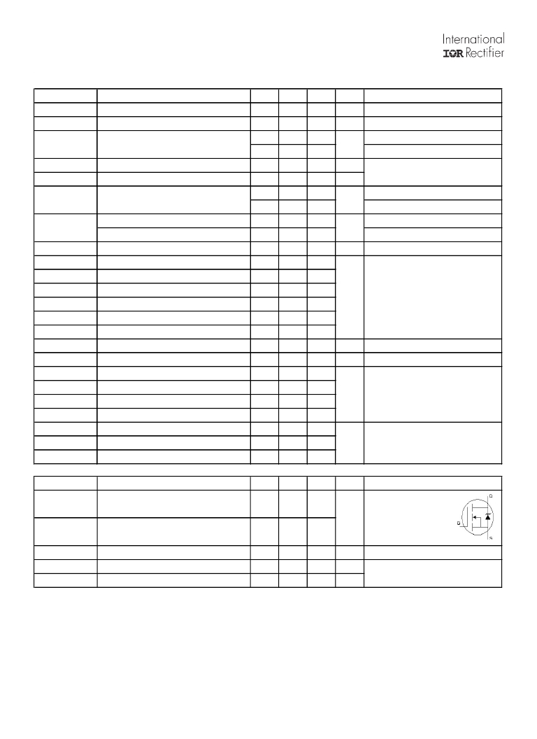
�Static� @� T� J� =� 25°C� (unless� otherwise� specified)�
�Parameter�
�Min.�
�Typ.� Max.� Units�
�Conditions�
�BV� DSS�
�Drain-to-Source� Breakdown� Voltage�
�40�
�–––�
�–––�
�V�
�V� GS� =� 0V,� I� D� =� 250μA�
�?Β� V� DSS� /� ?� T� J�
�Breakdown� Voltage� Temp.� Coefficient�
�–––�
�38�
�–––�
�mV/°C� Reference� to� 25°C,� I� D� =� 1mA�
�R� DS(on)�
�Static� Drain-to-Source� On-Resistance�
�–––�
�5.9�
�8.3�
�m� ?�
�V� GS� =� 10V,� I� D� =� 12.7A� i�
�–––�
�7.1�
�9.9�
�V� GS� =� 4.5V,� I� D� =� 10.2A� i�
�V� GS(th)�
�?� V� GS(th)� /� ?� T� J�
�I� DSS�
�Gate� Threshold� Voltage�
�Gate� Threshold� Voltage� Coefficient�
�Drain-to-Source� Leakage� Current�
�1.35�
�–––�
�–––�
�1.80�
�-5.5�
�–––�
�2.25�
�–––�
�1.0�
�V�
�mV/°C�
�μA�
�V� DS� =� V� GS� ,� I� D� =� 250μA�
�V� DS� =� 32V,� V� GS� =� 0V�
�–––�
�–––�
�150�
�V� DS� =� 32V,� V� GS� =� 0V,� T� J� =� 125°C�
�I� GSS�
�gfs�
�Q� g�
�Q� gs1�
�Q� gs2�
�Q� gd�
�Q� godr�
�Q� sw�
�Q� oss�
�Gate-to-Source� Forward� Leakage�
�Gate-to-Source� Reverse� Leakage�
�Forward� Transconductance�
�Total� Gate� Charge�
�Pre-Vth� Gate-to-Source� Charge�
�Post-Vth� Gate-to-Source� Charge�
�Gate-to-Drain� Charge�
�Gate� Charge� Overdrive�
�Switch� Charge� (Q� gs2� +� Q� gd� )�
�Output� Charge�
�–––�
�–––�
�71�
�–––�
�–––�
�–––�
�–––�
�–––�
�–––�
�–––�
�–––�
�–––�
�–––�
�19�
�5.9�
�1.4�
�6.0�
�5.7�
�7.4�
�9.5�
�100�
�-100�
�–––�
�29�
�–––�
�–––�
�–––�
�–––�
�–––�
�–––�
�nA�
�S�
�nC�
�nC�
�V� GS� =� 20V�
�V� GS� =� -20V�
�V� DS� =� 10V,� I� D� =� 10.2A�
�V� DS� =� 20V�
�V� GS� =� 4.5V�
�I� D� =� 10.2A�
�See� Fig.� 17�
�V� DS� =� 16V,� V� GS� =� 0V�
�R� G�
�t� d(on)�
�t� r�
�Gate� Resistance�
�Turn-On� Delay� Time�
�Rise� Time�
�–––�
�–––�
�–––�
�1.0�
�13�
�27�
�1.5�
�–––�
�–––�
�?�
�V� DD� =� 20V,� V� GS� =� 4.5V� i�
�I� D� =� 10.2A�
�t� d(off)�
�t� f�
�C� iss�
�C� oss�
�C� rss�
�Turn-Off� Delay� Time�
�Fall� Time�
�Input� Capacitance�
�Output� Capacitance�
�Reverse� Transfer� Capacitance�
�–––�
�–––�
�–––�
�–––�
�–––�
�18�
�3.6�
�2560�
�370�
�200�
�–––�
�–––�
�–––�
�–––�
�–––�
�ns�
�pF�
�Clamped� Inductive� Load�
�V� GS� =� 0V�
�V� DS� =� 20V�
�?� =� 1.0MHz�
�Diode� Characteristics�
�Parameter�
�Min.�
�Typ.� Max.� Units�
�Conditions�
�I� S�
�Continuous� Source� Current�
�–––�
�–––�
�53�
�MOSFET� symbol�
�(Body� Diode)�
�A�
�showing� the�
�I� SM�
�Pulsed� Source� Current�
�–––�
�–––�
�102�
�integral� reverse�
�(Body� Diode)�
�g�
�p-n� junction� diode.�
�V� SD�
�t� rr�
�Q� rr�
�Diode� Forward� Voltage�
�Reverse� Recovery� Time�
�Reverse� Recovery� Charge�
�–––�
�–––�
�–––�
�–––�
�15�
�5.5�
�1.0�
�23�
�8.3�
�V�
�ns�
�nC�
�T� J� =� 25°C,� I� S� =� 10.2A,� V� GS� =� 0V� i�
�T� J� =� 25°C,� I� F� =� 10.2A�
�di/dt� =� 100A/μs� i�
�Notes:�
�?� Repetitive� rating;� pulse� width� limited� by� max.� junction� temperature.�
�?� Pulse� width� ≤� 400μs;� duty� cycle� ≤� 2%.�
�2�
�www.irf.com�
�发布紧急采购,3分钟左右您将得到回复。
相关PDF资料
IRF6633TR1
MOSFET N-CH 20V 16A DIRECTFET-MP
IRF6644TR1
MOSFET N-CH 100V DIRECTFET-MN
IRF6645
MOSFET N-CH 100V DIRECTFET-SJ
IRF6655TR1
MOSFET N-CH 100V DIRECTFET-SH
IRF6665TR1
MOSFET N-CH 100V DIRECTFET-SH
IRF6668TR1
MOSFET N-CH 80V 55A DIRECTFET-MZ
IRF710STRLPBF
MOSFET N-CH 400V 2.0A D2PAK
IRF7201TR
MOSFET N-CH 30V 7.3A 8-SOIC
相关代理商/技术参数
IRF6614TR1PBF
功能描述:MOSFET MOSFT 40V 55A 8.3mOhm 19nC Qg RoHS:否 制造商:STMicroelectronics 晶体管极性:N-Channel 汲极/源极击穿电压:650 V 闸/源击穿电压:25 V 漏极连续电流:130 A 电阻汲极/源极 RDS(导通):0.014 Ohms 配置:Single 最大工作温度: 安装风格:Through Hole 封装 / 箱体:Max247 封装:Tube
IRF6614TR1PBF
制造商:International Rectifier 功能描述:MOSFET
IRF6614TRPBF
功能描述:MOSFET 40V 1 N-CH 5.9mOhm DirectFET 1.8Vgs RoHS:否 制造商:STMicroelectronics 晶体管极性:N-Channel 汲极/源极击穿电压:650 V 闸/源击穿电压:25 V 漏极连续电流:130 A 电阻汲极/源极 RDS(导通):0.014 Ohms 配置:Single 最大工作温度: 安装风格:Through Hole 封装 / 箱体:Max247 封装:Tube
IRF6616
功能描述:MOSFET 40V 1 N-CH 3.7mOhm DirectFET 1.8V Vgs RoHS:否 制造商:STMicroelectronics 晶体管极性:N-Channel 汲极/源极击穿电压:650 V 闸/源击穿电压:25 V 漏极连续电流:130 A 电阻汲极/源极 RDS(导通):0.014 Ohms 配置:Single 最大工作温度: 安装风格:Through Hole 封装 / 箱体:Max247 封装:Tube
IRF6616TR1
功能描述:MOSFET 40V 1 N-CH 3.7mOhm DirectFET 1.8V Vgs RoHS:否 制造商:STMicroelectronics 晶体管极性:N-Channel 汲极/源极击穿电压:650 V 闸/源击穿电压:25 V 漏极连续电流:130 A 电阻汲极/源极 RDS(导通):0.014 Ohms 配置:Single 最大工作温度: 安装风格:Through Hole 封装 / 箱体:Max247 封装:Tube
IRF6616TR1PBF
功能描述:MOSFET MOSFT 40V 106A 5.0mOhm 29nC Qg RoHS:否 制造商:STMicroelectronics 晶体管极性:N-Channel 汲极/源极击穿电压:650 V 闸/源击穿电压:25 V 漏极连续电流:130 A 电阻汲极/源极 RDS(导通):0.014 Ohms 配置:Single 最大工作温度: 安装风格:Through Hole 封装 / 箱体:Max247 封装:Tube
IRF6616TR1PBF
制造商:International Rectifier 功能描述:MOSFET
IRF6616TRPBF
功能描述:MOSFET 40V 1 N-CH 3.7mOhm DirectFET 1.8V Vgs RoHS:否 制造商:STMicroelectronics 晶体管极性:N-Channel 汲极/源极击穿电压:650 V 闸/源击穿电压:25 V 漏极连续电流:130 A 电阻汲极/源极 RDS(导通):0.014 Ohms 配置:Single 最大工作温度: 安装风格:Through Hole 封装 / 箱体:Max247 封装:Tube